TSMC builds 0.42nm interface to improve next-gen MoS2 transistors
Researchers from National Yang Ming Chiao Tung University and TSMC have developed a new interface design for atomically thin transistors. They created a 0.42-nanometre aluminium oxide layer between monolayer MoS2 and a hafnium oxide dielectric. The design helped the transistors maintain strong electrical control and carrier transport while using an extremely thin insulating layer.
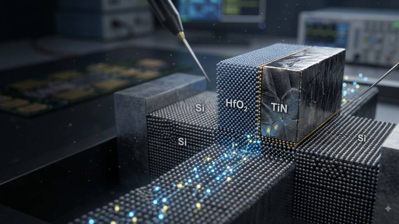
A research team from Taiwan's National Yang Ming Chiao Tung University and TSMC Corporate Research have developed a method to enhance transistors made from atomically thin materials. Their focus lies in the narrow interface region where two materials meet, which allows them to construct transistors with an ultra-thin insulating layer while preserving strong electrical performance.
Atomically thin semiconductors have been studied for over a decade due to their potential to create smaller, faster, and more energy-efficient transistors than conventional silicon-based devices. However, achieving optimal performance with these very thin transistors has proven challenging. The gate dielectric, an extremely thin insulating layer that controls electron movement, can suffer from issues at the material interface when made thinner.
The NYCU team collaborated with TSMC Corporate Research to address this problem by modifying the atomic interface between the semiconductor and the insulating layer. They utilized monolayer molybdenum disulfide (MoS2) as the semiconductor and placed an ultrathin epitaxial aluminium layer directly on it. Next, they oxidized the aluminium to create a 0.42-nanometre thick aluminium oxide layer, which acts as a buffer between MoS2 and the high-κ hafnium oxide gate dielectric.
This 0.42-nanometre aluminium oxide layer serves to smooth the surface, facilitating uniform growth of the hafnium oxide and minimizing unwanted electrical interactions between the two materials. The study, published in Nature Electronics, showcases that the atomic interface between materials can be as crucial as the choice of semiconductor or gate dielectric materials.
The researchers built short-channel top-gate transistors using CVD-grown monolayer MoS2 and achieved low leakage current, minimal hysteresis, and a maximum transconductance of 0.45 mS μm-1 with channel lengths of around 100 nanometres. These transistors demonstrated a combination of a very thin dielectric, strong electrical control, and maintained carrier transport, which has been difficult to achieve in atomically thin transistors.
The findings emphasize the growing significance of interfaces as transistor components shrink in size. When materials are only a few atomic layers thick, the interface between them can significantly impact device performance. Professor Tsung-En Lee, the study's corresponding author, stated that engineering these interfaces with atomic precision can unlock new possibilities for designing future semiconductor devices that would be challenging to achieve by altering the individual materials alone.
Written by urgent.news from Times of India's reporting — not their text. Machine-written — may contain errors; check the original before relying on it.