Researchers work out how to control 2D semiconductor growth for future chips
Korean boffins use oxygen to stop crystals forming in the wrong places, aiming to get tech to commercial sector by 2030
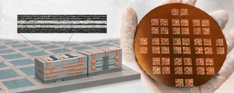
Researchers have developed a new method for controlling the growth of 2D semiconductor crystals, which could help address a major challenge in manufacturing next-generation chips at scale. The study, published in Nature, introduces a technique called spatially deterministic nucleation of 2D semiconductors by etching flux. This method uses an etching flux to suppress the formation of new crystals within each patterned growth region, except at the geometric center.
By doing so, the process encourages the formation of a single crystal in each region, potentially leading to more uniform and high-performance devices. The researchers successfully built working field-effect transistors using this method, achieving a high yield of 99.3 percent single crystals on a two-centimeter substrate. This advancement could pave the way for stacking 2D semiconductor devices on silicon chips, bringing logic and memory closer together and enabling more functions in a smaller area while reducing data transfer times and energy consumption.
Brief written by urgent.news from The Register's own syndicated text. Machine-written — may contain errors; check the original before relying on it.
This story
This is one outlet's version. Read the fullest account.