Researchers work out how to control 2D semiconductor growth for future chips
Korean boffins use oxygen to stop crystals forming in the wrong places, aiming to get tech to commercial sector by 2030
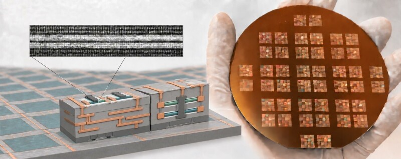
Scientists have devised a method to direct the growth of two-dimensional semiconductor crystals on a slab, a potential solution to a hurdle in mass-producing chips for the next generation, according to a paper published in the journal Nature on October 7. The study, titled "Spatially deterministic nucleation of 2D semiconductors by etching flux," was co-authored by researchers from KAIST and TDS Innovation, a South Korean startup.
The technique involves using an etching flux to inhibit the formation of new crystals throughout each patterned growth area, except at the center. Two-dimensional materials, which are atomically thin instead of literally two-dimensional, possess unique properties. Graphene, the most recognized example, is a single layer of carbon atoms but lacks an intrinsic band gap, making it unsuitable for standard switching transistors.
Certain transition-metal dichalcogenides (TMDs), like molybdenum disulfide, have a band gap and are being explored for use in future transistors and nanoscale devices. However, when grown on a wafer, 2D semiconductor crystals typically begin forming randomly, leading to multiple crystals and boundaries that degrade electrical performance.
The researchers developed an etching-flux-mediated single-centred nucleation (EF-SCN) process to encourage a single crystal to form in each patterned region. Oxygen released from an oxide barrier generates a lateral etching flux that curtails nucleation, except at the geometric center of the pattern. The team utilized this process to construct functional field-effect transistors (FETs), the fundamental components of modern chips.
They documented enhanced charge-carrier mobility, a metric of how easily charge moves through the material, as compared to previously reported results for selectively grown MoS₂ transistors. In an additional test across a two-centimeter substrate, the process yielded single crystals at 397 out of 400 patterned sites, a yield of 99.3 percent.
While this is not a demonstration of commercial chip production, it is a promising step towards scaling up. The co-CEO of TDS Innovation, co-author Kibum Kang, stated that stacking 2D semiconductor devices on silicon chips could bring logic and memory closer together, enabling more functions to be packed into a given area and reducing the time and energy spent moving data between them.
The startup also envisions using this ability to control where crystal growth begins to produce high-quality 2D single crystals uniformly where desired for next-generation semiconductors. Kang expects commercial use of 2D semiconductors around 2030, driven by increasing demand from AI, including physical AI and robotics. However, production timing will depend on further validation.
Written by urgent.news from The Register Science's reporting — not their text. Machine-written — may contain errors; check the original before relying on it.