Samsung chairman highlights chip packaging, visits Japanese unit
Samsung Electronics Executive Chairman Lee Jae-yong visited the company’s semiconductor advanced packaging technology laboratory in Japan, Sunday, pledging to continue expanding its research workforce there and develop the lab into a global R&D hub for next-generation packaging technologies. According to Samsung Electronics, Lee visited Advanced Package Lab (APL) in Yokohama and discussed with…
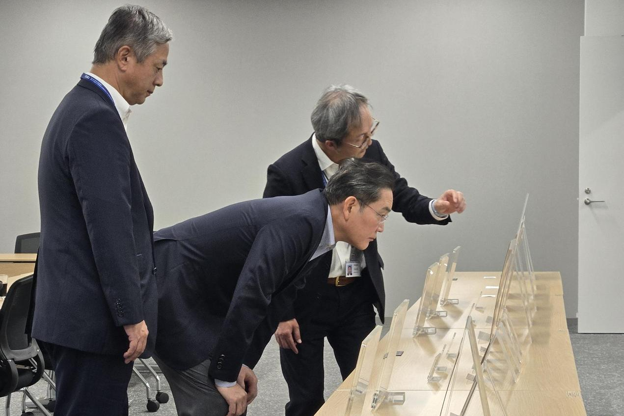
Samsung Electronics Executive Chairman Lee Jae-yong recently toured the company's semiconductor advanced packaging technology laboratory in Japan, pledging to bolster the research workforce and elevate the lab into a global R&D hub for next-generation packaging technologies. During his visit to the Advanced Package Lab (APL) in Yokohama, Lee engaged with researchers to discuss recent advancements in packaging materials and processes, as well as potential avenues to enhance collaboration between Japan's materials, parts, and equipment industries.
The Samsung executive emphasized the growing significance of advanced packaging technologies, particularly in the context of artificial intelligence (AI) processor chips. Established in 2023, the APL officially opened its doors in September of that year. In 2024, Samsung Electronics is set to invest 40 billion yen ($254 million) over a five-year period to establish its research infrastructure in Japan and bolster its competitiveness in advanced packaging technologies.
The APL specializes in the development and manufacture of advanced packaging materials and processes, with a focus on creating smaller, faster, and more energy-efficient chips. Lee's visit underscores Samsung's commitment to staying at the forefront of the rapidly evolving semiconductor industry, as Japan's robust materials and manufacturing sectors present a strategic opportunity for partnership and innovation.
Written by urgent.news from The Korea Times's reporting — not their text. Machine-written — may contain errors; check the original before relying on it.
This story
This is one outlet's version. Read the fullest account.
- Samsung chairman highlights chip packaging, visits Japanese unit koreatimes.co.kr