Samsung chairman highlights chip packaging, visits Japanese unit
Samsung Electronics Executive Chairman Lee Jae-yong visited the company’s semiconductor advanced packaging technology laboratory in Japan, Sunday, pledging to continue expanding its research workforce there and develop the lab into a global R&D hub for next-generation packaging technologies. According to Samsung Electronics, Lee visited Advanced Package Lab (APL) in Yokohama and discussed with…
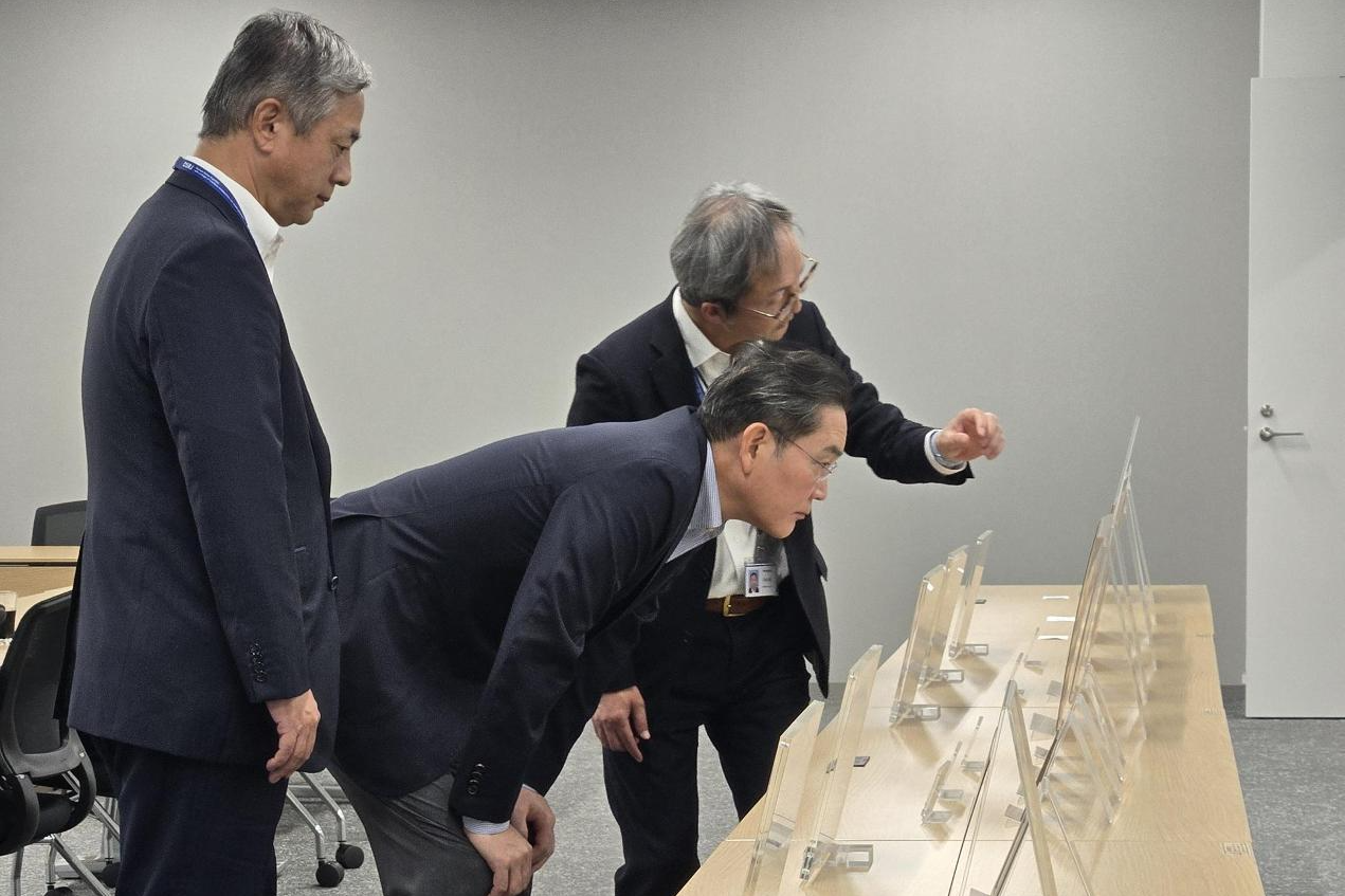
Samsung Electronics Executive Chairman Lee Jae-yong visited the company's Advanced Package Lab (APL) in Yokohama, Japan, on Sunday to highlight the importance of chip packaging research. During his visit, Lee stressed the significance of securing advanced packaging technologies for artificial intelligence (AI) processor chips and pledged to continue expanding the lab's research workforce.
Samsung Electronics has committed to investing 40 billion yen ($254 million) over five years to establish its research infrastructure in Japan and strengthen its competitiveness in advanced packaging technologies.
Brief written by urgent.news from The Korea Times's own syndicated text. Machine-written — may contain errors; check the original before relying on it.
Also reported by 1 other outlet
- Samsung chairman highlights chip packaging, visits Japanese unit koreatimes.co.kr