ASML eyes hybrid bonding, report finds, as Chinese firms adopt chip packaging technique
Dutch semiconductor equipment giant ASML is expanding into next-generation hybrid bonding, a technique that creates dense electrical connections by directly joining chips or silicon wafers, according to a new report. Major Chinese companies are also adopting the technology to improve chip performance. ASML submitted 27 patent families related to hybrid bonding tools between December 2022 and…
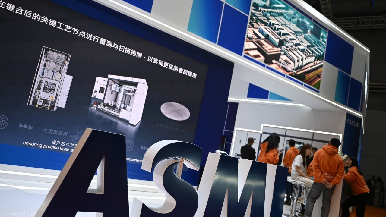
ASML, a leading Dutch semiconductor equipment manufacturer, is exploring hybrid bonding technology, a method that enables dense electrical connections by directly joining chips or silicon wafers. Major Chinese firms are also adopting this technique to enhance chip performance, according to a report by SemiAnalysis. Between December 2022 and November 2024, ASML filed 27 patent families related to hybrid bonding tools, potentially indicating a broader scope of progress than initially disclosed.
The company is reportedly collaborating with Dutch tech firms Prodrive Technologies and VDL ETG to develop the architecture for a hybrid bonder. ASML CEO Christophe Fouquet hinted at ongoing efforts to support customers in hybrid bonding during an April earnings call. Hybrid bonding allows for ultra-high-density electrical connections and is considered a significant trend in chipmaking.
Chinese tech giants Huawei and ChangXin Memory Technologies have utilized hybrid bonding to improve performance amid US-led export restrictions on advanced semiconductor equipment. The technique can reduce thermal resistance in high-bandwidth memory stacks by up to 30%, potentially lowering cooling requirements. However, China remains reliant on imported hybrid bonding equipment, with domestic manufacturers striving to reduce the gap.
Written by urgent.news from South China Morning Post's reporting — not their text. Machine-written — may contain errors; check the original before relying on it.