Samsung, ASML team up on next-generation semiconductor manufacturing technology
SEOUL, Sept. 8 (Yonha) -- Samsung Electronics Co. said Tuesday that it has joine...
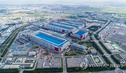
Samsung Electronics has joined forces with ASML, a Netherlands-based semiconductor equipment manufacturer, to develop cutting-edge semiconductor manufacturing technologies. The partnership focuses on advancing 12-inch photomask technology, which will replace the widely-used 6-inch format. This collaboration aims to accelerate the development of technologies that meet the growing demands for performance and efficiency in advanced semiconductor manufacturing.
The new technology is expected to significantly boost fab productivity and reduce chipmaking costs, particularly as demand for artificial intelligence (AI) chips continues to surge. ASML's CEO, Menno van Roon, emphasized the importance of the partnership in supporting technological innovation throughout the semiconductor value chain.
Samsung's CEO, Jun Young-hyun, highlighted the company's commitment to further strengthening the collaboration with ASML. He stated that this partnership will lay the foundation for the next generation of AI and semiconductor innovation.
In a groundbreaking move, Samsung plans to introduce ASML's High NA Extreme Ultraviolet (EUV) lithography technology into the high-volume manufacturing of dynamic random-access memory (DRAM) by 2028. This technology will provide improved resolution, simplify the fabrication process, and enhance manufacturing efficiency. By extending the DRAM scaling road map, High NA EUV is expected to play a crucial role in the semiconductor industry's future.
Written by urgent.news from Yonhap News's reporting — not their text. Machine-written — may contain errors; check the original before relying on it.
This story
This is one outlet's version. Read the fullest account.
- Samsung, ASML expand partnership to introduce next-gen lithography by 2028 koreatimes.co.kr
- ASML draws Samsung, TSMC to next-gen EUV machines techinasia.com