SK hynix to hold groundbreaking ceremony for Indiana chip packaging plant on Aug. 27
SEOUL, Aug. 12 (Yonhap) -- SK hynix Inc. will hold a formal groundbreaking cerem...
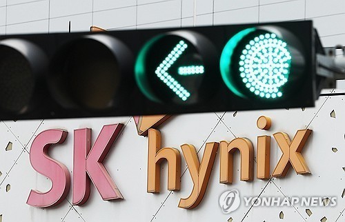
SK hynix Inc. is set to mark the occasion of its new semiconductor packaging plant in Indiana with a groundbreaking ceremony on August 27, according to industry sources. The South Korean chipmaker has announced plans to invest $3.87 billion in its first U.S. advanced packaging and research and development facility in West Lafayette, Indiana.
This plant will focus on producing high bandwidth memory (HBM) chips designed for artificial intelligence (AI) applications. Notable attendees at the ceremony are expected to include SK hynix CEO Kwak Noh-jung, as well as CEOs and officials from several major technology companies. SK Group Chairman Chey Tae-won may also make an appearance, and there are reports suggesting that Nvidia Corp. CEO Jensen Huang might attend as well.
SK hynix and Nvidia have been collaborating on global AI data center projects and memory chip supply, with Chey and Huang engaging in frequent meetings over the past year.
Written by urgent.news from Yonhap News's reporting — not their text. Machine-written — may contain errors; check the original before relying on it.