A new way to watch heat move through electronics
MIT researchers can now precisely measure how heat moves through multilayered materials like computer chips.
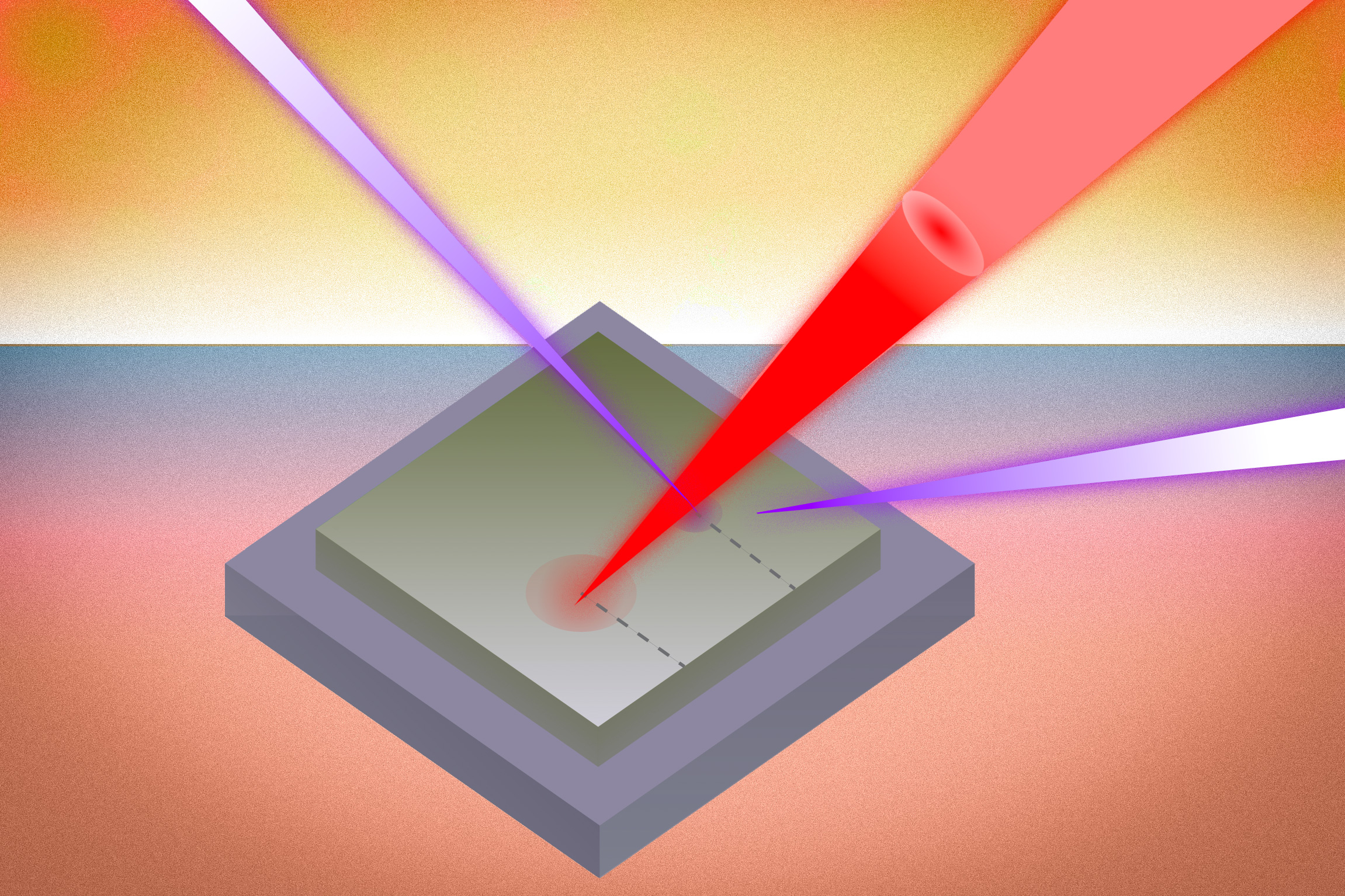
As computer chips continue to shrink in size and power, managing their heat output is becoming an increasingly critical issue. Traditional methods for measuring heat flow are limited when it comes to analyzing multilayered devices, such as modern electronics that power our daily lives. A team of researchers from MIT has developed a novel technique that combines X-rays capable of penetrating multiple layers with laser pulses to deliver heat.
By employing this innovative method, the researchers were able to precisely measure heat transfer within a promising material for transistors and flexible electronics. Their observations revealed that even a single micron-scale defect in the device could lead to a significant reduction in its ability to transfer heat, with a surprising fourfold decrease in thermal conductivity at the defect's location.
Furthermore, the study found that the defect caused heat to disperse unevenly, with a greater ease of movement in one direction compared to the other.
The implications of this groundbreaking approach could be far-reaching for the electronics industry, particularly in the development of more powerful and compact devices. Some examples include AI applications, wearable technology, and clean energy systems. Mingda Li, an associate professor at MIT and co-corresponding author of the research paper, emphasizes the importance of tackling overheating issues, stating that it has become a major bottleneck in device performance.
Traditional diagnostic techniques fall short in their ability to observe heat flow at the micro- or nanometer scale.
The researchers' new method offers a promising step forward in addressing this challenge, as it allows for detailed analysis of heat carriers and the identification of factors contributing to device failures. The technique uses electron pulses and ultrafast X-rays to measure changes in material strain at the atomic level while the X-rays penetrate multiple layers of the material, providing a clearer picture of heat propagation across interfaces.
The researchers applied their technique to a test device featuring a layer of gallium nitride atop silicon, a material combination commonly studied for its heat-conducting properties. Their findings demonstrated a fourfold reduction in heat dissipation due to a defect on the device, with a 25 percent drop in heat dissipation across materials as well.
As the demand for more powerful computers and electronics continues to grow, this novel approach to heat measurement could play a crucial role in helping researchers design better devices and avoid local hotspots. By observing heat transfer at the nanoscale, scientists can gain valuable insights into the underlying causes of overheating and develop strategies to enhance the overall efficiency of electronic systems.
Written by urgent.news from MIT News Research's reporting — not their text. Machine-written — may contain errors; check the original before relying on it.