Samsung showcases chip 3D architecture strategy at SEMICON Taiwan
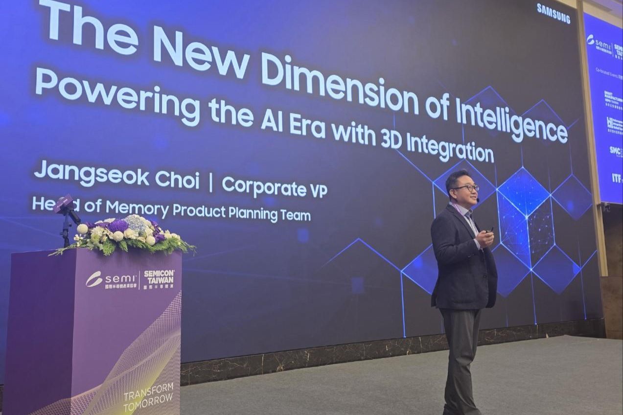
Samsung Electronics on Tuesday showcased its 3D architecture strategy to break through current limitations in memory chip manufacturing during SEMICON Taiwan 2026, an international exhibition covering semiconductor design, manufacturing, testing and packaging. According to the company, Samsung Electronics Device Solutions Vice President Choi Jang-seok delivered a keynote speech at the Memory…
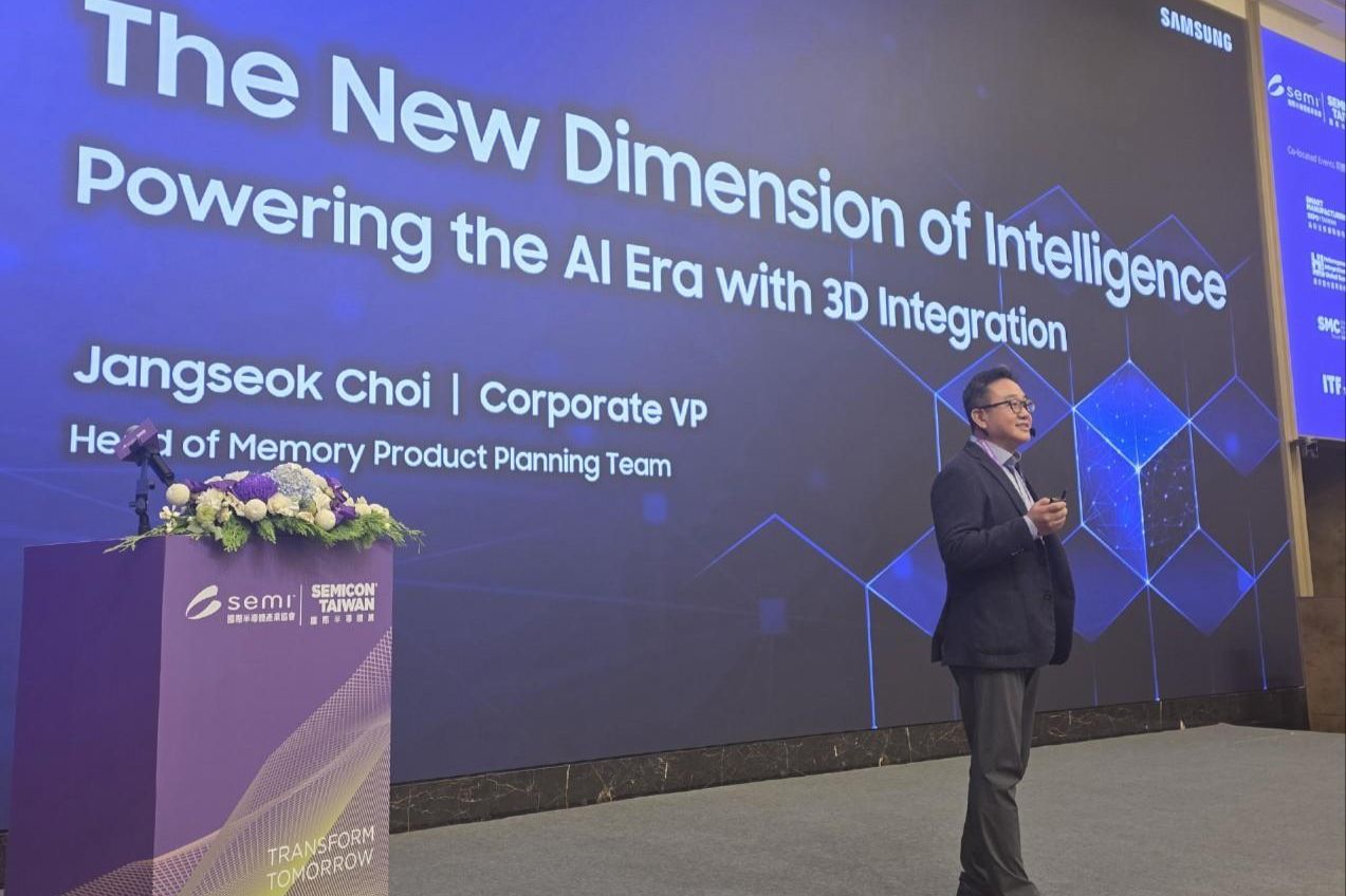
Samsung Electronics presented its innovative 3D architecture strategy at the SEMICON Taiwan 2026 exhibition, aimed at overcoming current constraints in memory chip manufacturing. The company's vice president for device solutions, Choi Jang-seok, delivered a keynote address at the Memory Executive Summit, an event previewing SEMICON Taiwan 2026, set to run for three days beginning on Wednesday.
Choi's presentation highlighted Samsung's "CUBE" strategy, which integrates 3D technologies across all stages of memory chip manufacturing. This approach seeks to enhance memory capacity, utilization, bandwidth, and energy efficiency. The 3D architecture Samsung is adopting involves stacking chip dies or other components vertically, thereby reducing the physical distance data needs to travel and increasing the number of data pathways.
This vertical stacking method, as Choi explained, is where the term "3D architecture" originates. Unlike traditional memory chips where chips or memory dies are placed side by side on a two-dimensional plane, Samsung's strategy involves building these components upwards in layers. This design choice not only optimizes space but also significantly boosts energy efficiency. The high-bandwidth memory (HBM) is one example of the advanced memory solutions Samsung plans to develop using this 3D architecture strategy.
Written by urgent.news from The Korea Times's reporting — not their text. Machine-written — may contain errors; check the original before relying on it.
This story
This is one outlet's version. Read the fullest account.
- Samsung showcases chip 3D architecture strategy at SEMICON Taiwan koreatimes.co.kr
- Semicon 2.0: What is India’s new Rs 1.27 lakh-crore push for chip design? indianexpress.com