Samsung reveals next-gen memory with stacked HBM and 400-layer NAND
At the Future of Memory and Storage 2026 conference in Santa Clara, California, the company laid out a roadmap built around three main technologies: a new Bonding V-NAND architecture with more than 400 layers, a concept for vertically stacked high-bandwidth memory called zHBM, and a next-generation NAND approach called zNAND-O.... Read Entire Article
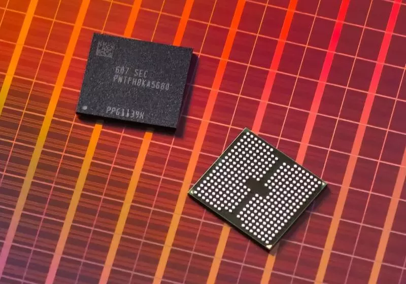
Samsung is unveiling cutting-edge memory technologies to bolster its AI initiatives, as showcased at the Future of Memory and Storage 2026 conference in California. The focus lies on three key technologies: Bonding V-NAND with over 400 layers, vertically stacked high-bandwidth memory (zHBM), and the next-generation NAND solution (zNAND-O). These advancements aim to cater to both massive AI training workloads in data centers and edge AI applications demanding swift data processing and minimal power consumption.
A standout feature is zHBM, a novel arrangement of high-bandwidth memory. Contrary to conventional setups where HBM is positioned adjacent to AI processors, zHBM integrates the memory directly atop AI accelerators. This strategic positioning reduces the physical distance data must traverse, thereby enhancing bandwidth and power efficiency for large-scale AI operations.
Samsung anticipates zHBM to deliver roughly eight times the performance of the existing HBM5 standard. By leveraging wafer bonding, the company projects zHBM to achieve more than ten times the memory density of HBM5, while simultaneously improving energy efficiency by threefold and reducing thermal resistance by more than half. This enables the creation of high-capacity, high-bandwidth systems that are more stable and easier to cool, thereby optimizing AI hardware design.
Another noteworthy technology is zNAND-O, a high-performance NAND solution tailored for edge AI applications. Currently under development in four and eight-layer iterations, this innovative NAND approach combines high space efficiency, enhanced input/output performance, and low latency to facilitate real-time, data-intensive AI tasks closer to the source of data generation.
Positioned between traditional mass-storage NAND and memory products specifically designed for rapid inference and local processing, zNAND-O strikes a balance between these two categories. The conference also spotlighted V10 BV-NAND, Samsung's first Bonding V-NAND architecture, which employs wafer bonding to stack memory cells, thereby increasing storage density and performance while simultaneously reducing power consumption.
V10 BV-NAND boasts a 58% increase in memory density compared to its V9 generation, alongside improved read, write, and input/output performance, catering to future AI systems and applications necessitating high performance and high capacity.
Written by urgent.news from TechSpot's reporting — not their text. Machine-written — may contain errors; check the original before relying on it.