Samsung chief visits Advanced Package Lab in Japan
SEOUL, Nov. 1 (Yonhap) -- Samsung Electronics Co. Chairman Lee Jae-yong visited ...
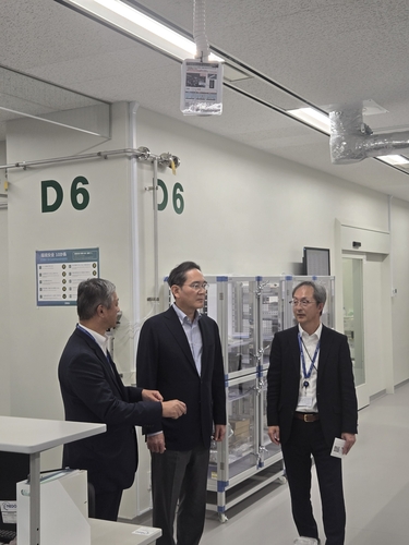
Samsung Electronics Chairman Lee Jae-yong visited the company's Advanced Package Lab (APL) in Yokohama, Japan, on November 1. The APL, opened in September, serves as a global R&D hub for technologies that improve the performance of artificial intelligence (AI) chips. During his visit, Lee Jae-yong met with APL researchers to discuss advancements in key materials and process technologies for advanced semiconductor packaging.
He emphasized the importance of securing these technologies to maintain competitiveness in the semiconductor industry amidst the AI era. Samsung established the APL in 2023, investing 350 billion won (approximately US$262 million) in R&D over five years.
Written by urgent.news from Yonhap News's reporting — not their text. Machine-written — may contain errors; check the original before relying on it.