Applied Materials’ $5 billion AI lab aims to cut chip development time in half—and restore Silicon Valley’s edge
Applied Materials, the leading maker of chipmaking equipment, officially unveiled its EPIC chip R&D center with partner companies including Intel, Micron, SK Hynix, and Samsung Electronics.
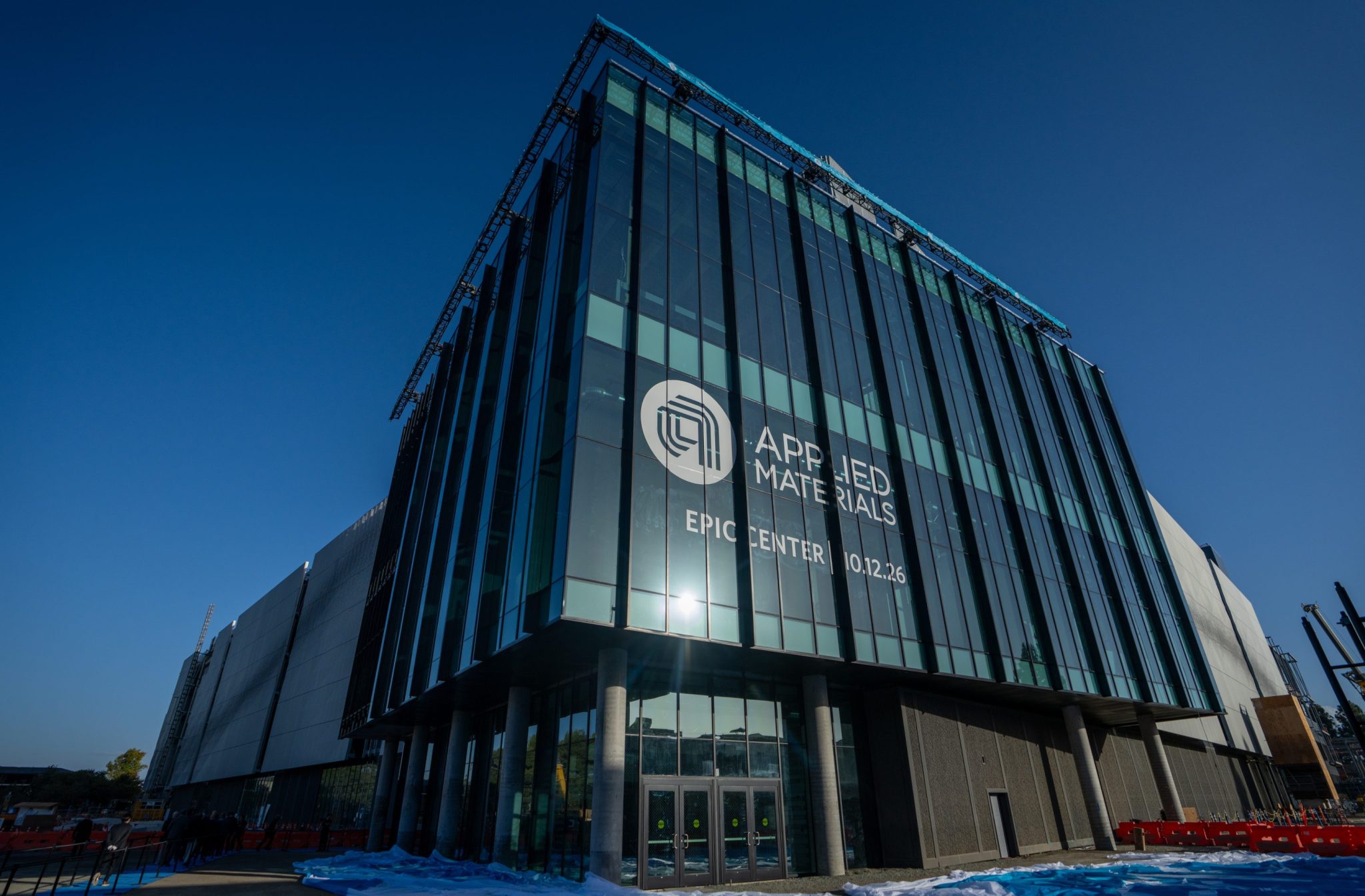
Silicon Valley, home to world-renowned tech giants such as Apple, Alphabet, and Meta, has historically struggled when it comes to creating the physical facilities necessary for chip development. The area's skyline is dominated by low-slung buildings and office parks, rather than the towering chip fabrication plants common overseas.
In a surprising move, Applied Materials, the world's largest chipmaking equipment producer, has unveiled a monumental new facility aimed at reversing this trend. The $5 billion EPIC (Extreme Performance Integrated Computing) research and development center, located in Sunnyvale, California, is the largest investment of its kind in the United States.
Partnering with industry leaders like Intel, TSMC, Micron, SK Hynix, and Samsung, Applied Materials aims to accelerate chip development and help restore Silicon Valley's technological edge. The 600,000-square-foot facility, spanning the size of three football fields, features state-of-the-art clean rooms where researchers can work with advanced chipmaking equipment.
By co-locating innovators and providing early access to cutting-edge technology, Applied Materials expects to cut the typical "concept to commercialization" timeframe from 10 to 12 years down to as little as six years. This collaboration not only has the potential to speed up the development of AI models but also to keep Silicon Valley at the forefront of chip technology, despite the U.S. government's restrictions on advanced chip manufacturing equipment sales to China.
Written by urgent.news from Fortune's reporting — not their text. Machine-written — may contain errors; check the original before relying on it.