Russian firm completes country's first 130nm-capable chipmaking tool, trails modern equipment by 25 years
ZNTC completes development of Russia's first 130nm-capable lithography stepper, which could be used to produce chips sometimes late this decade, or rather early next.
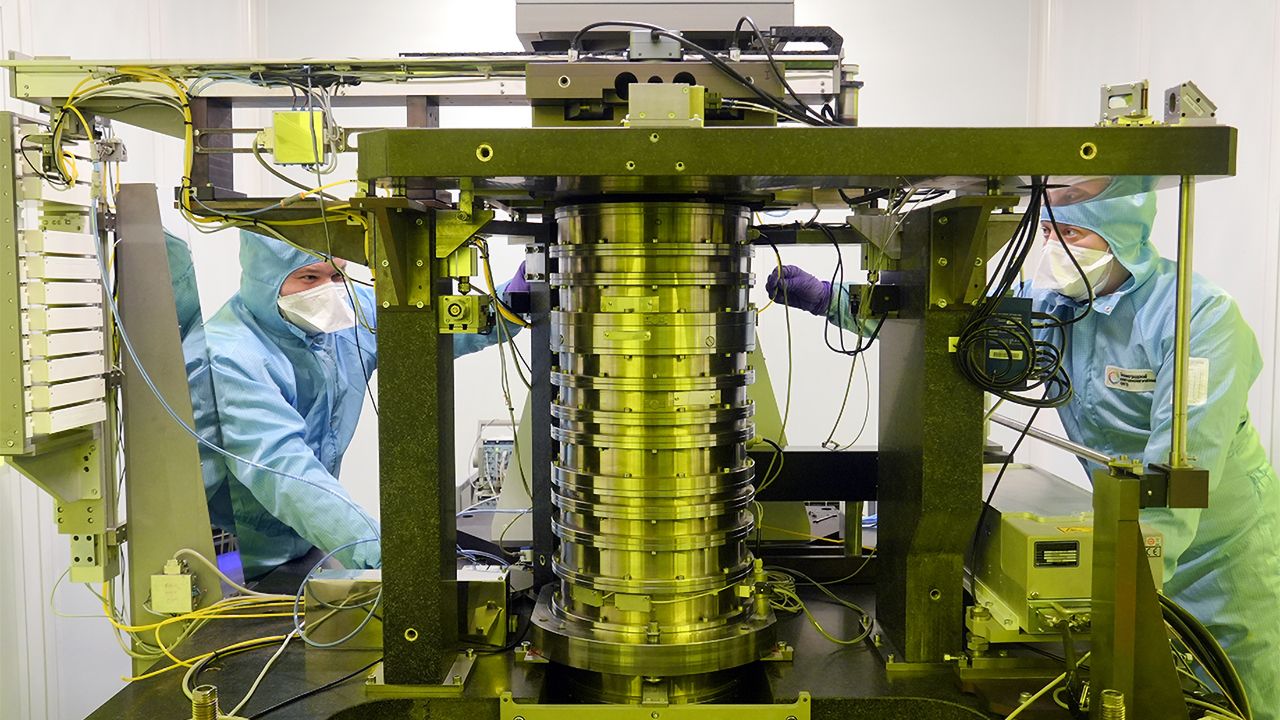
The Russian firm Zelenograd Nanotechnology Center (ZNTC) has recently finished the third development stage of its inaugural lithography tool, capable of processing 200-millimeter wafers using a 130nm process technology. The tool is presently undergoing internal testing and has yet to be deployed at a manufacturing facility for mass chip production.
According to blogger Dmitrii Kuznetsov, this device is the first Russian lithography system with 130nm capability, featuring components manufactured domestically. The creation of this domestically developed photolithography system represents a significant milestone for Russia's microelectronics sector, showcasing the country's engineering expertise in this field.
The project was jointly developed by ZNTC and Belarus-based Planar, with Lasers developed by Lassard. Russia's Ministry of Industry and Trade invested around $70 million in the entire development program. The cost of a single 130nm-capable ZNTC stepper, including its laser light source, is approximately $7.3 million, which is significantly more expensive than the $3.1 million list price of ASML's PAS 5500/150 stepper from 2001.
Despite these advancements, the Russian stepper is still years away from being utilized for actual chip production, estimated to be around 2029 at the earliest.
Written by urgent.news from Tom's Hardware's reporting — not their text. Machine-written — may contain errors; check the original before relying on it.