TSMC, Samsung, and Intel shore up support with ASML to deploy larger High-NA EUV photomasks — 6×12-inch photomask transition may take years despite unified effort
ASML, Intel, Samsung, and TSMC back development of 6×12-inch to build large processors using High-NA EUV lithography systems without stitching.
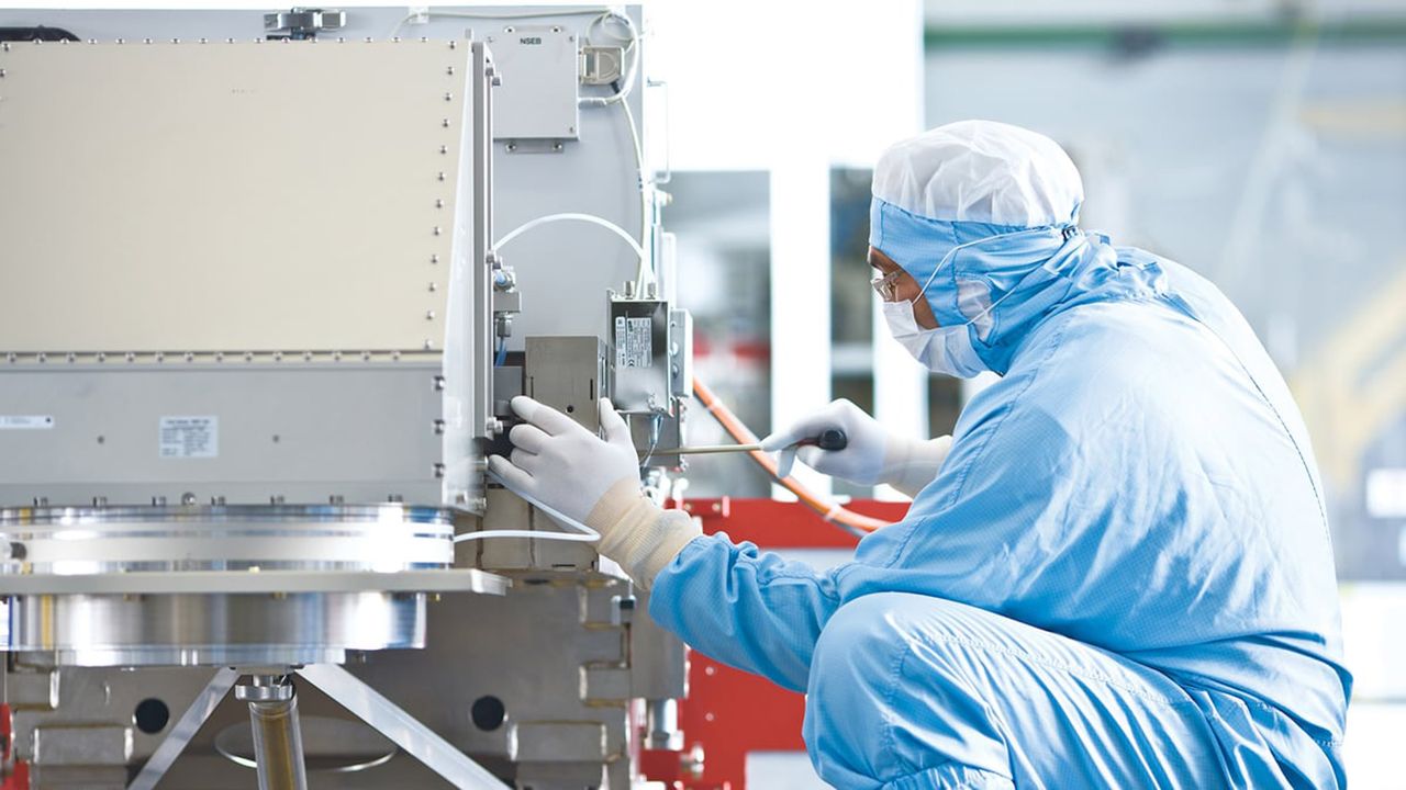
ASML, Intel, Samsung, and TSMC are joining forces to transition to 6×12-inch photomasks, a move crucial for implementing High-NA Extreme Ultraviolet (EUV) lithography. Larger photomasks allow for printing bigger chips in a single pass, avoiding the need to combine smaller designs, as ASML explained in a recent press release. While such collaboration is not unprecedented, it's uncommon when facing an industry-wide challenge.
This situation mirrors previous transitions, such as the 450-mm wafer and EUV efforts, where chipmakers set aside their rivalry to advance the industry. High-NA EUV lithography, with a numerical aperture of 0.55, offers an 8nm single-exposure resolution, compared to 13nm for 0.33-NA EUV scanners. This enhanced resolution enables smaller, denser features to be patterned in a single exposure, reducing mask and process steps, shortening manufacturing cycle times, and potentially improving pattern fidelity and yields.
Nonetheless, the transition comes with tradeoffs. High-NA EUV uses 4X/8X anamorphic optics, making the same mask expose only a 26×16.5 mm half-field, unlike conventional systems that expose a 26×33 mm full-field. This necessitates stitching or splitting large dies into multi-chiplet designs, leading to reduced throughput, additional design rules, and the risk of alignment errors causing defects and yield loss.
The industry will require new 6×12-inch photomasks, which would necessitate significant changes to mask-making, handling, and lithography infrastructure. Mask-blank suppliers, mask shops, and fabs would need to adapt to the larger format, while ASML would have to modify its High-NA EUV scanners and related tools. The transition to 6×12-inch masks is an ongoing industry effort involving ASML, Intel, Samsung, and TSMC and may take years to complete.
Written by urgent.news from Tom's Hardware's reporting — not their text. Machine-written — may contain errors; check the original before relying on it.