ASML and TSMC want bigger masks for smaller chips
Industry push aims to eliminate stitching constraints and ready high-NA EUV systems for production by 2033
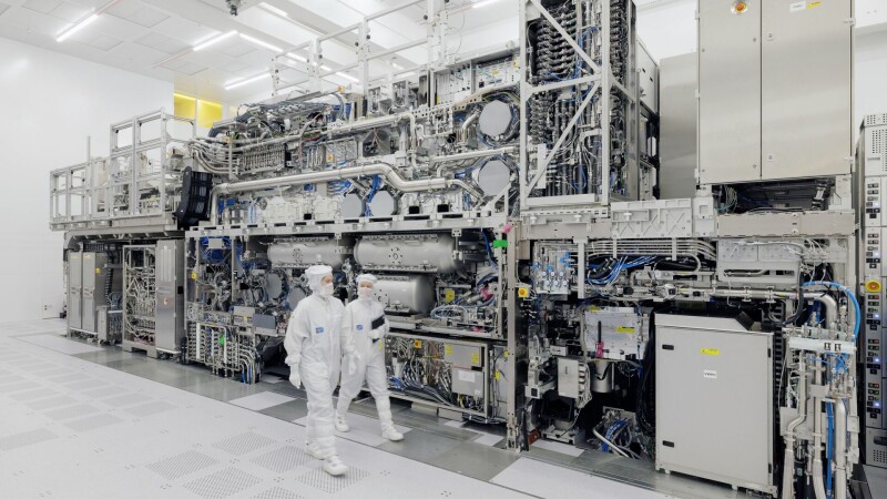
ASML and leading chipmaker TSMC have embarked on a collaborative effort to transition to 12-inch photomasks in the industry, aiming to lower costs and overcome challenges posed by high-NA EUV lithography. ASML, the sole commercial supplier of EUV lithography systems, has partnered with TSMC to drive the shift to larger-format masks for extreme ultraviolet (EUV) lithography.
Other industry players, including Intel Foundry and Samsung Electronics, have expressed their support for this initiative. The plan is to establish a 12-inch mask pilot line by 2031 and have the necessary lithography systems ready for advanced node production by 2033. While high-NA EUV lithography will initially be introduced using current 6-inch masks, moving to 12-inch masks could boost fab productivity, reduce costs, and eliminate stitching constraints.
This shift is driven by the anamorphic optical design adopted by ASML for its initial high-NA EUV machines, which allowed chipmakers to continue using existing 6-inch masks. However, this approach has resulted in reduced exposure fields, necessitating larger masks to restore the full exposure field as the industry pursues denser chips, smaller process nodes, and more energy-efficient devices.
ASML president and CEO Christophe Fouquet expects the adoption of high-NA EUV to progress along the device scaling roadmap, with the transition from 6-inch to 12-inch masks enabling increased scanner productivity and supporting the demand for smaller, faster, and more efficient chips. TSMC, which has not yet employed high-NA EUV in its 2 nm process, plans to deploy the technology for advanced nodes beginning in 2030.
Intel Foundry and Samsung Electronics have also signaled their support for the initiative, with plans to enable the transition to 6x12-inch masks and introduce ASML's high-NA EUV technology into high-volume DRAM manufacturing by 2028. IDC senior research director Andrew Buss emphasized the challenges posed by high-NA EUV, noting that reticle stitching and chiplet designs can help mitigate these issues.
However, he stressed that the move to 6 x 12-inch photomasks is a necessary step, comparable to the industry's transition from 200 mm to 300 mm wafers, and that broad industry participation is essential for a successful transition.
Written by urgent.news from The Register's reporting — not their text. Machine-written — may contain errors; check the original before relying on it.
Also reported by 1 other outlet
- ASML and TSMC want bigger masks for smaller chips theregister.com