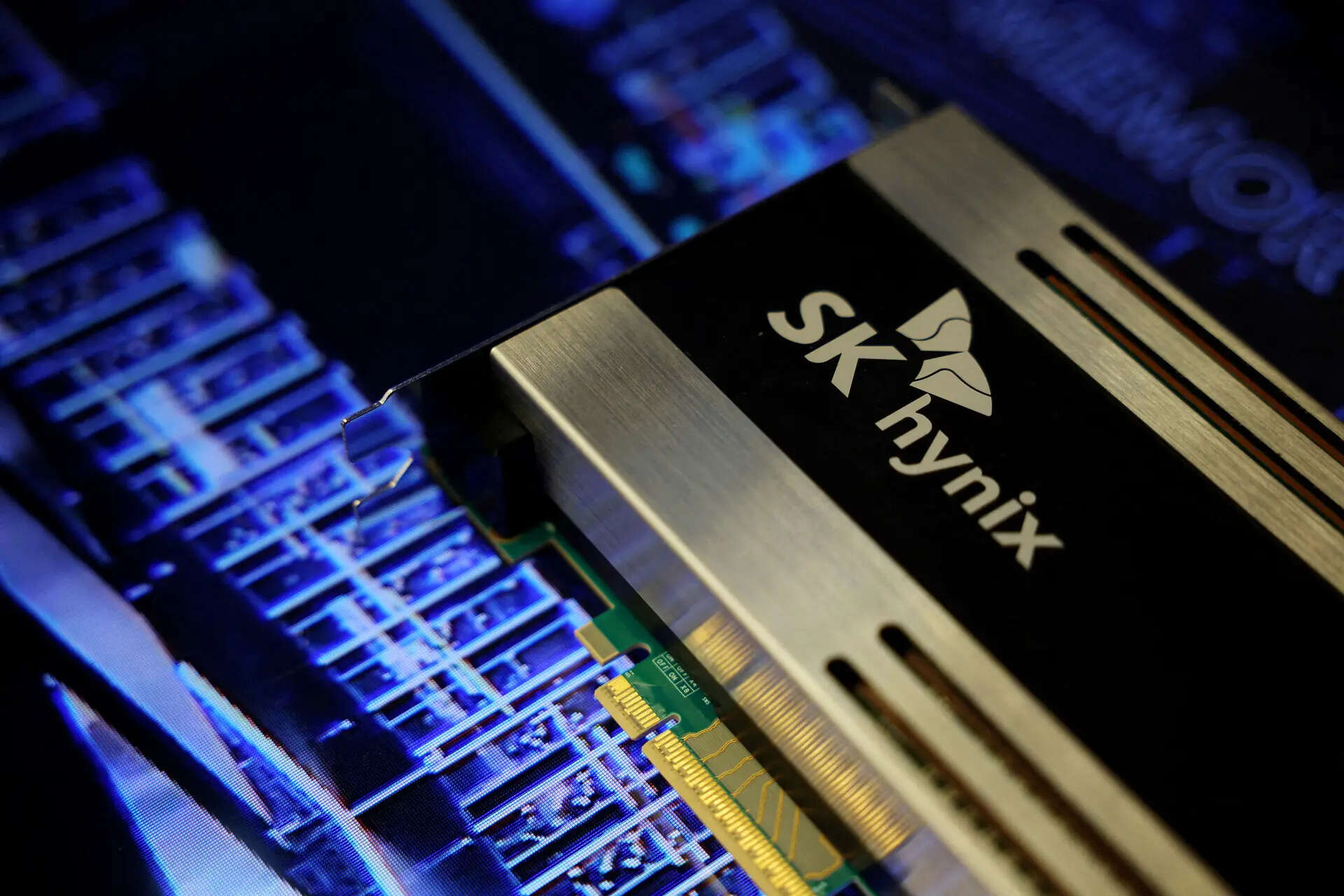
[르포] 미 ‘전공정’ 압박 속 첫삽… SK하이닉스, ‘메이드 인 USA HBM’ 승부수
On the 26th (local time), a significant event took place at SK Hynix's semiconductor factory construction site in West Lafayette, Indiana. Kim Hyun-jung, the project-team leader for the Indiana Puff construction project, posed a question to his team: what is the most significant difference between building a semiconductor factory in Korea and the United States?
He explained that in Korea, heavy semiconductor equipment is placed on a solid foundation, while here, the ground is nearly devoid of foundation, requiring stronger, deeper, and more multiple file placements. Kim Hyun-jung stated, "The differences in culture, language, environment, and perception are great, making each day new."
The site, once a paddy field, now houses massive concrete pillars and steel beams rising above a vast expanse of flat land, serving as the foundation for the clean room to be built on the second floor. These pillars will support the heavy equipment, suppressing even the slightest vibrations, unlike a regular building, which is much more compact.
Kim Hyun-jung reported that the overall project efficiency is around 7%, with the foundational construction efficiency at about 15%, progressing smoothly. "From next year's peak period, when electrical and mechanical work starts, we expect to increase the workforce by up to 3,000 people daily." The 'Indiana Puff' site, SK Hynix's first semiconductor production facility in the United States, was officially inaugurated on the 27th at Purdue University's Hallerway Stadium.
With an investment of over $4.8 billion (approximately 5.3 trillion won), the large-scale project will construct a cutting-edge high-bandwidth memory (HBM) packaging production line and research and development facilities on a 5.4 million square meter plot. The attention drawn by this inauguration was largely due to the United States' increasing pressure on Korean enterprises to produce memory chips domestically, in line with the CHIPS Act.
However, SK Hynix's Indiana Puff is distinct from the United States' demand for 'memory chip local production (wafer manufacturing) within the United States.' This facility will import Korean-made wafers, assemble the chips, and complete the high-bandwidth memory locally through advanced packaging. CEO Gwang No-jung of SK Hynix announced at the ceremony that they aim to achieve production capacity equivalent to tens of millions of units annually, positioning Indiana as a crucial hub for 'made in USA high-bandwidth memory' supply.
The extensive effort goes beyond just the construction of the factory; they are also prioritizing local sourcing, using as many American-made materials as possible for the foundation and major materials. SK Hynix's entry into the U.S. market with this facility will serve as a test bed for future expansion decisions in the country, as CEO Gwang No-jung has stated that they will consider additional memory production facilities in the U.S. based on labor acquisition, supply chain establishment, and favorable business conditions such as tax incentives and financial assistance.
Written by urgent.news from Hankyoreh's reporting — not their text. Machine-written — may contain errors; check the original before relying on it.