High Bandwidth Flash gets first technical specification for AI data centers
A year ago, SanDisk and SK Hynix announced a collaboration to develop a common standard for the High Bandwidth Flash (HBF) project. The new type of memory is designed to improve performance and power efficiency in AI data centers and can now be implemented in new data center projects thanks... Read Entire Article
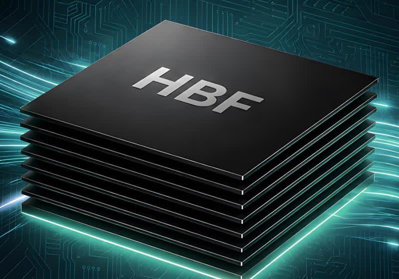
High Bandwidth Flash, or HBF, has achieved its first technical specification, paving the way for its adoption in AI data center projects. Two major memory manufacturers, SanDisk and SK Hynix, began collaborating on the HBF standard in 2025. The new memory type aims to boost performance and power efficiency in AI data centers. The Open Compute Project now hosts the HBF technical specification, which is accessible for free use in custom data center designs or server architectures.
HBF integrates the vast storage capacity of NAND flash chips with high-bandwidth data rates, similar to those found in High Bandwidth Memory products. It features eight vertically stacked HBF layers, offering a theoretical capacity of up to 4TB per chip. The specification outlines system interface, electrical requirements, performance expectations, and other technical guidelines necessary for integrating HBF into custom designs.
It also includes a software user guide detailing read and write operations. This milestone is crucial for data center operators and system builders, as it offers a practical solution for placing high-capacity memory and compute units closer to accelerators, fostering more flexible AI architectures.
Written by urgent.news from TechSpot's reporting — not their text. Machine-written — may contain errors; check the original before relying on it.